

 Image 1 of 9
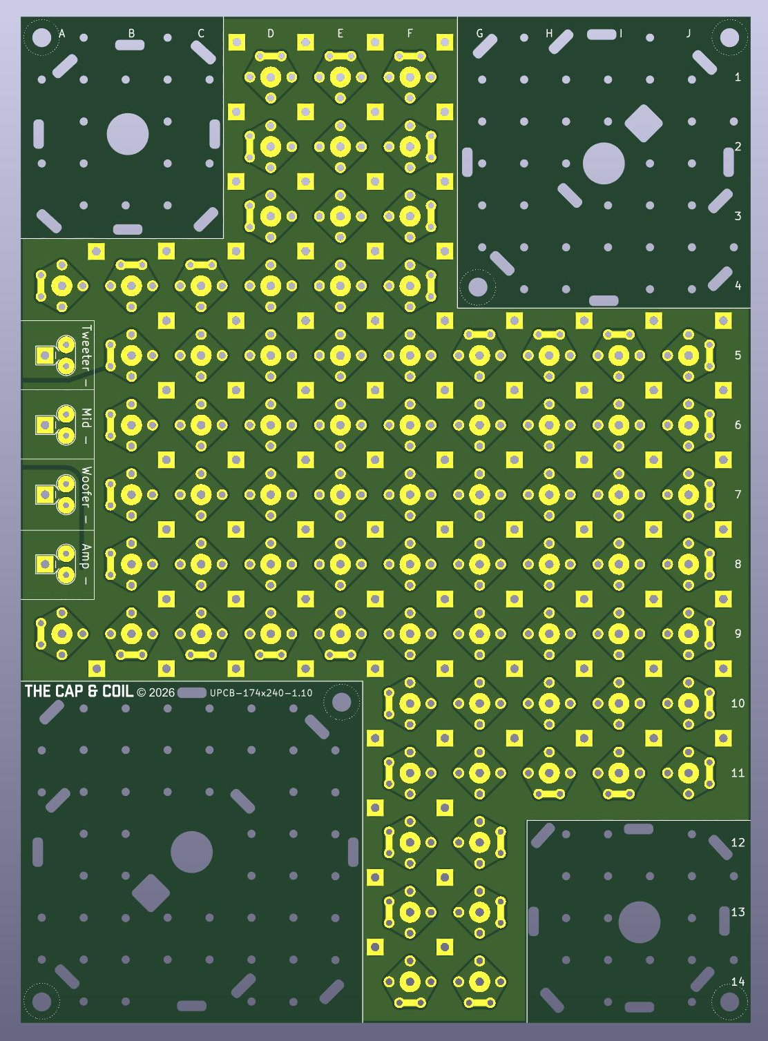 Image 2 of 9
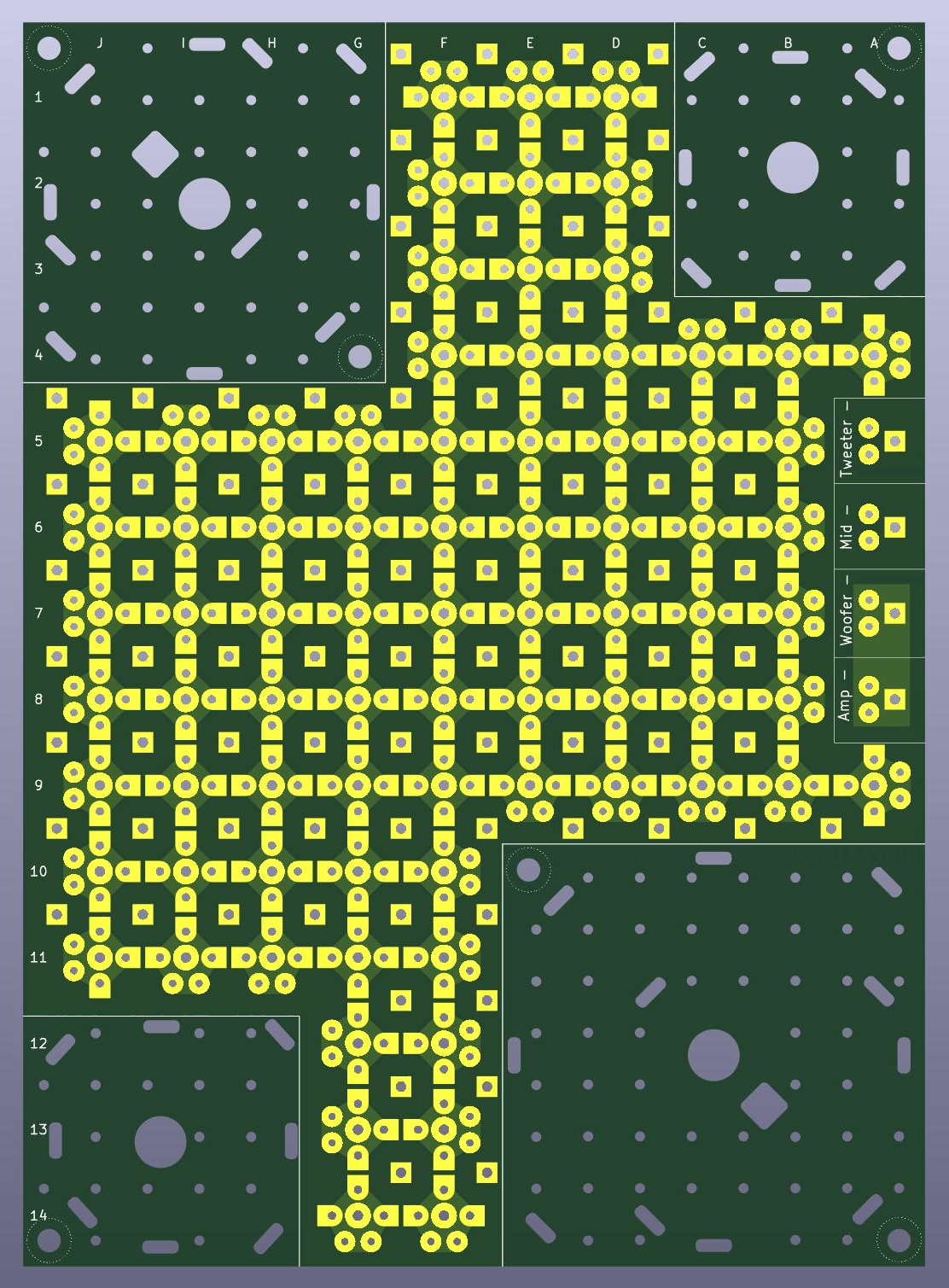 Image 3 of 9
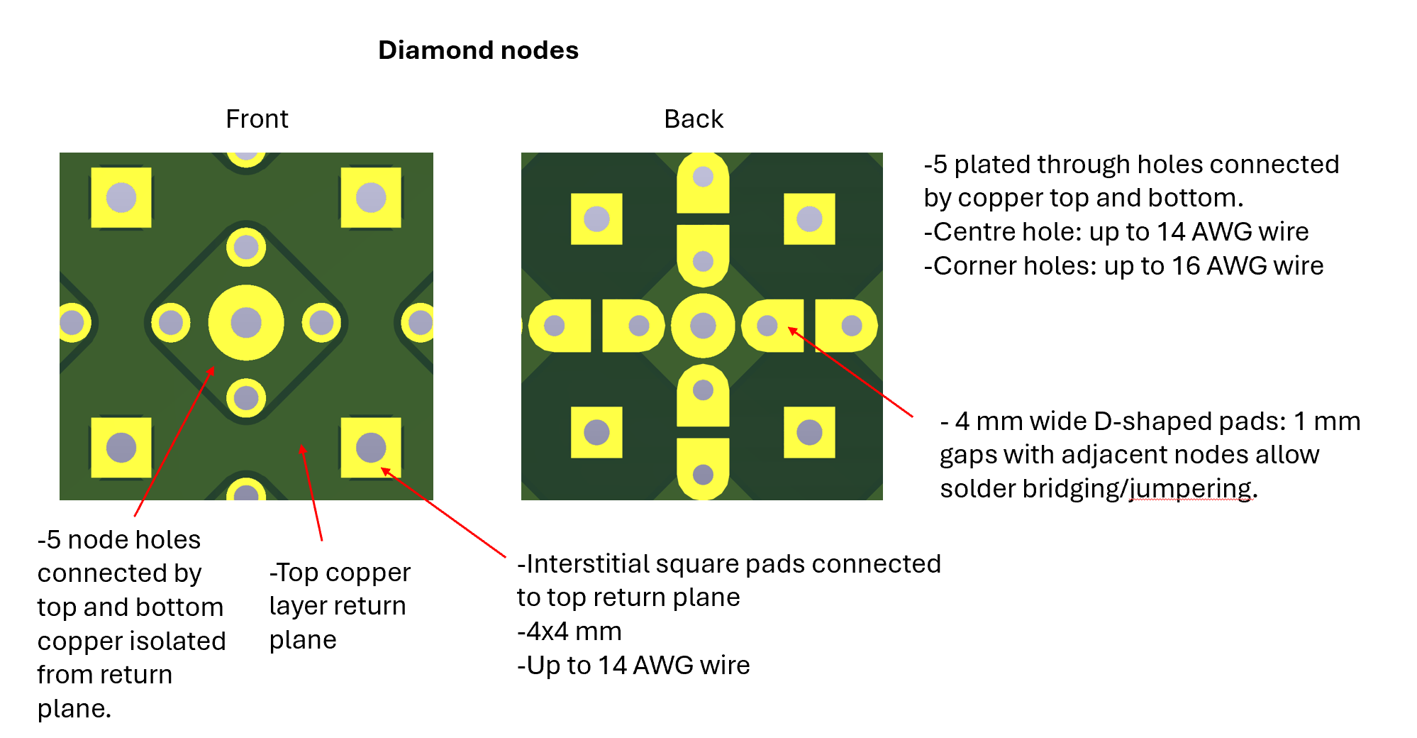 Image 4 of 9
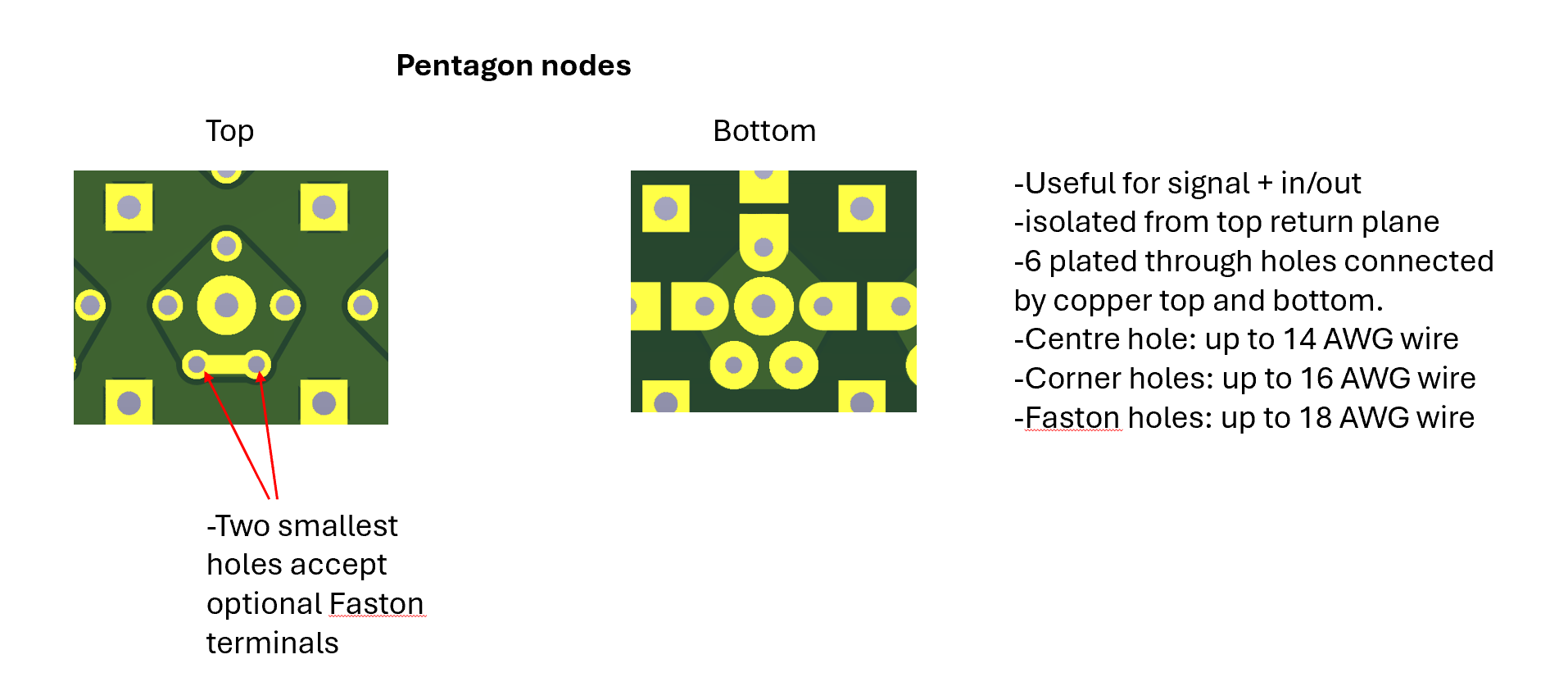 Image 5 of 9
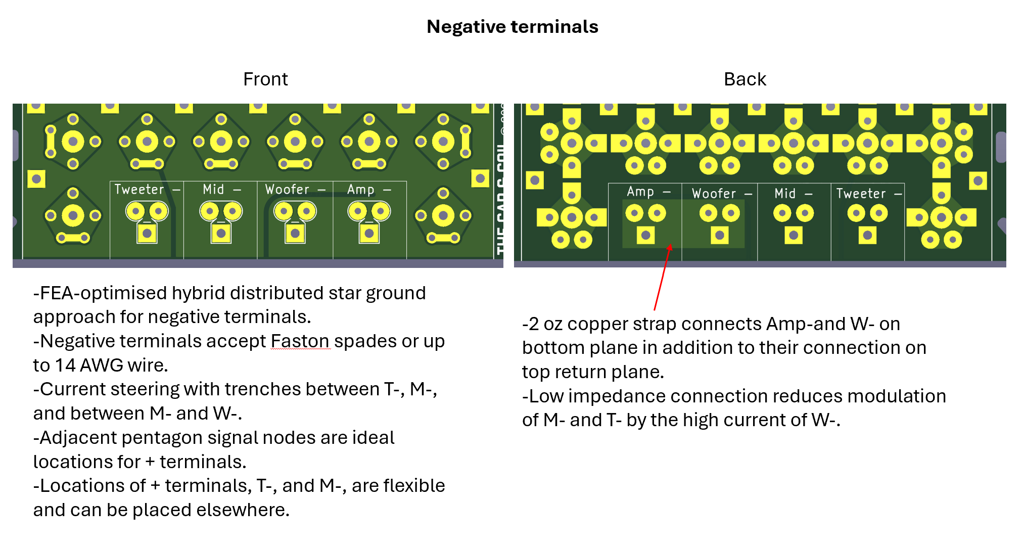 Image 6 of 9
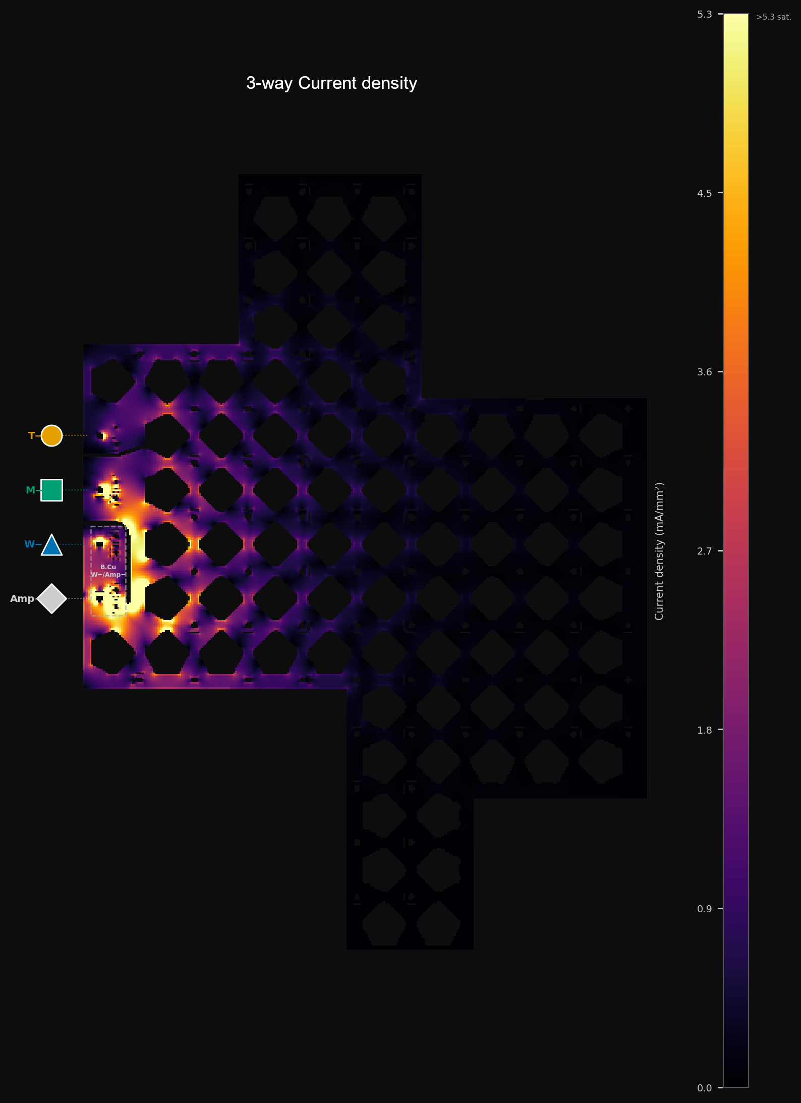 Image 7 of 9
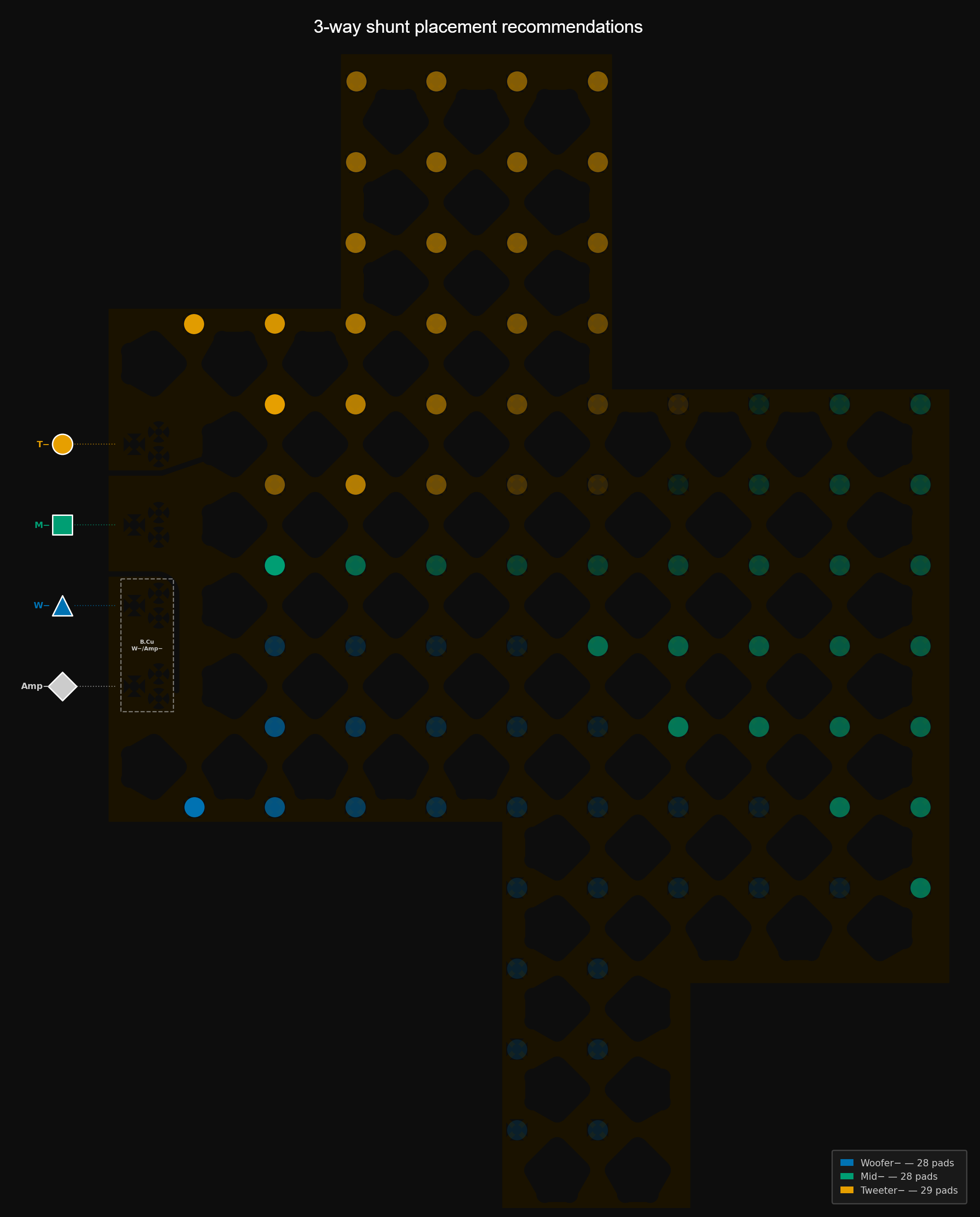 Image 8 of 9
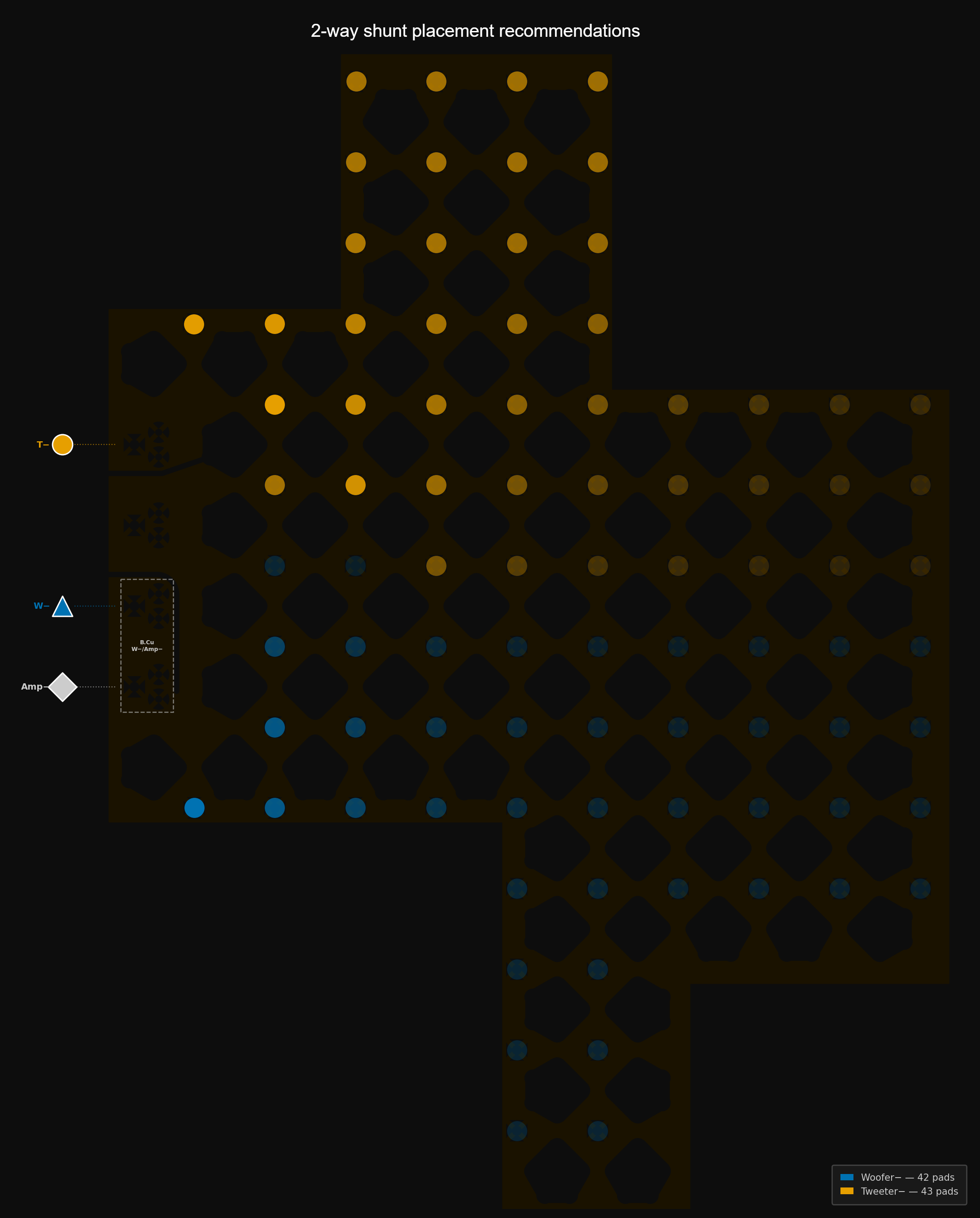 Image 9 of 9
Universal crossover PCB
● For 2- and 3-way passive crossovers ● Faster and easier to build than point-to-point ● Infinitely more flexible than topology-prescriptive PCBs ● Electrical performance optimised by Finite Element Analysis (FEA) ● Provided with FEA-guided user strategies
The problem with point-to-point
Getting a crossover design right takes substantial effort. The topology is deliberate, the values are all set, and the filter behaviour is exactly where you want it — all to achieve exactly the sound you’re going for. What you want now is a crossover build you can trust: consistent from joint to joint, repeatable from build to build, with the knowledge that what came off the workbench matches what you designed.
Point-to-point wiring is how most crossovers get built — and it works. But it introduces a problem that no amount of care fully solves: variability. Hand-soldered joints vary — in resistance, in mechanical strength, in long-term reliability. You can’t see the difference between a good joint and a marginal one, and there’s no reliable way to confirm that every connection in a finished assembly is equal to every other. For a one-off build, that uncertainty lingers. For production, it compounds: a crossover built on a Monday may not be electrically identical to one built on a Friday. A carefully designed speaker deserves better than that.
Topology-prescriptive PCBs help — but only so far
Commercial crossover PCBs improve on point-to-point in geometry and repeatability. The trade-off is flexibility: fixed positions for capacitors and inductors but only one architecture baked into the traces. That suits a design you never intend to change — but even a proven published crossover can be implemented better, and any serious refinement means bodge wires or cutting traces. The board also can’t accommodate topology changes: a different filter order, a Zobel network, baffle step correction, or a notch filter all require working around a layout that wasn’t designed for them.
Many commercial boards also use 1 oz copper — twice the return plane impedance of 2 oz, with every voltage drop and coupling figure scaled accordingly. It’s a reasonable cost trade-off for a fixed design, but it leaves performance on the table.
We’ve built crossovers both ways. We know what it feels like to finish a point-to-point build and wonder whether every connection is as good as it looks — and whether the next build will be the same. The UPCB-174x240 was designed to erase that doubt: a foundation that makes every build consistent, traceable, and worthy of the design behind it. It was developed in consultation with professional speaker designers and the DIY community, because the same problems show up in both worlds.
Designed with FEA, the board’s results are objectively robust. Subjectively, it is a pleasure flowing solder onto gold plated pads, compared to maybe or maybe not flowing solder perfectly between leads in a point-to-point build.
The UPCB-174x240
Getting started is straightforward. Download the user guide free at capandcoil.com.au. It covers layout principles, return pad placement, and the electrical analysis behind the design, so you can plan your build with confidence before a component is placed. Then lay out your design on the lettered and numbered grid: components go where the design needs them, not where a fixed layout allows them. Any 2- or 3-way passive crossover topology that fits the board can be built on it. Then build. Thread leads through from the front, solder on the back, and arrive at a finished assembly that is rigid, repeatable, and electrically predictable — identical to every other build from the same layout.
Physical features
Signal nodes in a solid return plane
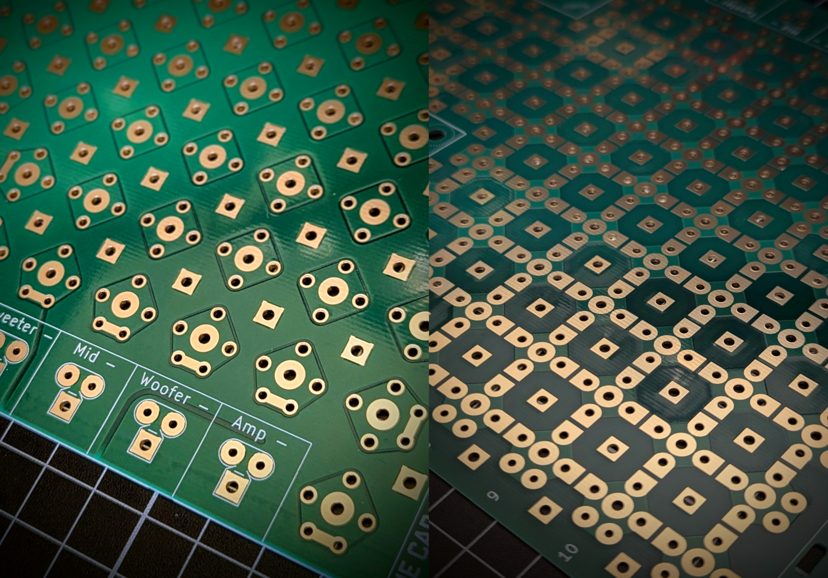
The front copper layer is a continuous 2 oz return plane. Signal nodes are isolated islands in this plane — groups of five or six through-holes on a 16.6 mm lettered and numbered grid. Thread leads through from the front, solder on the back. Multiple components share a node; adjacent nodes bridge via D-shaped back pads to suit any lead spacing. Place your components where your design needs them, not where a pre-designed prescriptive PCB allows them. Your layout is reproducible and its electrical characteristics are predictable before you solder the first joint.
Two node types
Diamond nodes (five holes) occupy the central grid. Pentagon nodes (six holes) sit along the board edges, with a pair of holes sized for optional 6.35 mm Faston terminals. Both types of nodes work identically for soldered connections.
Copper-free inductor zones
The four corner regions are copper-free inductor zones. Copper beneath an inductor increases ESR and reduces inductance — removing it keeps your inductors behaving according to your design. Each inductor zone includes cable tie slots for flat and upright orientations, M4 board mounting holes, and a 10 mm grid of unplated holes if you want to connect capacitors or resistors by point-to-point connections or turrets in those areas. Flat and upright zones sit on opposite corners to prevent inductor-to-inductor coupling.
2 oz copper, ENIG pads
Both layers are 2 oz (70 μm) copper with gold (ENIG) pads. The 2 oz copper halves return plane impedance compared to standard 1 oz boards, which is critical to electrical performance. ENIG pads solder beautifully, are lead-free, and have a much longer shelf-life than HASL pads.
Mechanical robustness
Once assembled, the board is a rigid, unified structure. Components are anchored to copper pads and heavy inductors are supported through the inductor zones. You can transport it, install it, pull it for service, and hand it to someone else without worrying about it. In a free-form build, unsupported component weight stresses joints over time, and a finished assembly requires more care in handling. The board fits through an 8 inch woofer hole and suits any cabinet with a screwed-on back panel. Smaller versions are under development.
Electrical performance
Return plane, not return wire
Resistance from Amp− to the most distant driver return connector is under 2.2 mΩ. At 1 W into 8 Ω, the maximum ground voltage at the tweeter connector is −62.6 dBV — comparable to the noise floor of a professional reel-to-reel recorder at 7½ ips. The woofer’s return current, carrying 70% of the power in a typical 2-way, modulates the tweeter’s ground reference at −65.7 dBV. For comparison, a single 10 cm run of 18 AWG hookup wire contributes −58.0 dBV at the same reference level — worse than the board’s entire return path. Every driver shares that same low-impedance foundation.
Hybrid distributed star ground
The ideal crossover ground is a star: all driver returns meeting at a single point, so no return current from one driver can influence another’s path. Point-to-point wiring a true star is entirely achievable, though it adds complexity and long runs can introduce their own problems. The UPCB-174x240 approaches the same result differently: return pads are distributed throughout the plane, so return currents enter the ground system locally. The plane’s low impedance keeps voltage differences across it small — in the millivolt range at normal signal levels — and each driver’s current occupies a distinct zone, with boundaries set by terminal positions, so woofer return current stays in the woofer region, not the tweeter region. Placing shunt components on return pads within each driver’s zone minimises cross-contamination between drivers. This zone separation is consistent and repeatable across every build.
Mid− and Tweeter− can be repositioned to any return pad to deliberately shift zone boundaries to suit your component layout.
Dedicated woofer return path
The woofer draws more current than any other driver, and that current has to return somewhere. A solid copper zone on the back of the board bridges Amp− and Woofer− directly, without thermal relief, carrying approximately 69% of the woofer’s return current. That cuts current density on the front-layer plane between those terminals by more than half. The driver doing the most work gets its own dedicated path — so it doesn’t compromise the rest of your ground system.
Low and predictable parasitics
Parasitic resistance, inductance, and capacitance aren’t on your schematic — but they’re in every physical circuit, shifting filter frequencies and degrading slopes. The UPCB-174x240 addresses all three: resistance through 2 oz copper and a full return plane; inductance through short, wide current paths and the two-dimensional distribution of the plane, which minimises effective loop area; layout variability through the fixed grid, so parasitic behaviour is consistent and predictable from build to build. What you simulated is what you get.
For designers and manufacturers alike
Whether you’re building one crossover or a hundred, the same things matter: joints you can trust, layouts you can reproduce, and a build process that doesn’t introduce variability the design never intended. The UPCB-174x240 was designed for professional production and works equally well for the hobbyist who demands the same standard from a one-off build.
The lettered grid makes layout fast to learn and easy to follow. Builds are reproducible — the same layout produces the same electrical result, every time — and the board is rigid enough to handle, install, and service without concern. When the design evolves, the new version builds on the same board with the same process. No new tooling, no new learning curve.
● For 2- and 3-way passive crossovers ● Faster and easier to build than point-to-point ● Infinitely more flexible than topology-prescriptive PCBs ● Electrical performance optimised by Finite Element Analysis (FEA) ● Provided with FEA-guided user strategies
The problem with point-to-point
Getting a crossover design right takes substantial effort. The topology is deliberate, the values are all set, and the filter behaviour is exactly where you want it — all to achieve exactly the sound you’re going for. What you want now is a crossover build you can trust: consistent from joint to joint, repeatable from build to build, with the knowledge that what came off the workbench matches what you designed.
Point-to-point wiring is how most crossovers get built — and it works. But it introduces a problem that no amount of care fully solves: variability. Hand-soldered joints vary — in resistance, in mechanical strength, in long-term reliability. You can’t see the difference between a good joint and a marginal one, and there’s no reliable way to confirm that every connection in a finished assembly is equal to every other. For a one-off build, that uncertainty lingers. For production, it compounds: a crossover built on a Monday may not be electrically identical to one built on a Friday. A carefully designed speaker deserves better than that.
Topology-prescriptive PCBs help — but only so far
Commercial crossover PCBs improve on point-to-point in geometry and repeatability. The trade-off is flexibility: fixed positions for capacitors and inductors but only one architecture baked into the traces. That suits a design you never intend to change — but even a proven published crossover can be implemented better, and any serious refinement means bodge wires or cutting traces. The board also can’t accommodate topology changes: a different filter order, a Zobel network, baffle step correction, or a notch filter all require working around a layout that wasn’t designed for them.
Many commercial boards also use 1 oz copper — twice the return plane impedance of 2 oz, with every voltage drop and coupling figure scaled accordingly. It’s a reasonable cost trade-off for a fixed design, but it leaves performance on the table.
We’ve built crossovers both ways. We know what it feels like to finish a point-to-point build and wonder whether every connection is as good as it looks — and whether the next build will be the same. The UPCB-174x240 was designed to erase that doubt: a foundation that makes every build consistent, traceable, and worthy of the design behind it. It was developed in consultation with professional speaker designers and the DIY community, because the same problems show up in both worlds.
Designed with FEA, the board’s results are objectively robust. Subjectively, it is a pleasure flowing solder onto gold plated pads, compared to maybe or maybe not flowing solder perfectly between leads in a point-to-point build.
The UPCB-174x240
Getting started is straightforward. Download the user guide free at capandcoil.com.au. It covers layout principles, return pad placement, and the electrical analysis behind the design, so you can plan your build with confidence before a component is placed. Then lay out your design on the lettered and numbered grid: components go where the design needs them, not where a fixed layout allows them. Any 2- or 3-way passive crossover topology that fits the board can be built on it. Then build. Thread leads through from the front, solder on the back, and arrive at a finished assembly that is rigid, repeatable, and electrically predictable — identical to every other build from the same layout.
Physical features
Signal nodes in a solid return plane
The front copper layer is a continuous 2 oz return plane. Signal nodes are isolated islands in this plane — groups of five or six through-holes on a 16.6 mm lettered and numbered grid. Thread leads through from the front, solder on the back. Multiple components share a node; adjacent nodes bridge via D-shaped back pads to suit any lead spacing. Place your components where your design needs them, not where a pre-designed prescriptive PCB allows them. Your layout is reproducible and its electrical characteristics are predictable before you solder the first joint.
Two node types
Diamond nodes (five holes) occupy the central grid. Pentagon nodes (six holes) sit along the board edges, with a pair of holes sized for optional 6.35 mm Faston terminals. Both types of nodes work identically for soldered connections.
Copper-free inductor zones
The four corner regions are copper-free inductor zones. Copper beneath an inductor increases ESR and reduces inductance — removing it keeps your inductors behaving according to your design. Each inductor zone includes cable tie slots for flat and upright orientations, M4 board mounting holes, and a 10 mm grid of unplated holes if you want to connect capacitors or resistors by point-to-point connections or turrets in those areas. Flat and upright zones sit on opposite corners to prevent inductor-to-inductor coupling.
2 oz copper, ENIG pads
Both layers are 2 oz (70 μm) copper with gold (ENIG) pads. The 2 oz copper halves return plane impedance compared to standard 1 oz boards, which is critical to electrical performance. ENIG pads solder beautifully, are lead-free, and have a much longer shelf-life than HASL pads.
Mechanical robustness
Once assembled, the board is a rigid, unified structure. Components are anchored to copper pads and heavy inductors are supported through the inductor zones. You can transport it, install it, pull it for service, and hand it to someone else without worrying about it. In a free-form build, unsupported component weight stresses joints over time, and a finished assembly requires more care in handling. The board fits through an 8 inch woofer hole and suits any cabinet with a screwed-on back panel. Smaller versions are under development.
Electrical performance
Return plane, not return wire
Resistance from Amp− to the most distant driver return connector is under 2.2 mΩ. At 1 W into 8 Ω, the maximum ground voltage at the tweeter connector is −62.6 dBV — comparable to the noise floor of a professional reel-to-reel recorder at 7½ ips. The woofer’s return current, carrying 70% of the power in a typical 2-way, modulates the tweeter’s ground reference at −65.7 dBV. For comparison, a single 10 cm run of 18 AWG hookup wire contributes −58.0 dBV at the same reference level — worse than the board’s entire return path. Every driver shares that same low-impedance foundation.
Hybrid distributed star ground
The ideal crossover ground is a star: all driver returns meeting at a single point, so no return current from one driver can influence another’s path. Point-to-point wiring a true star is entirely achievable, though it adds complexity and long runs can introduce their own problems. The UPCB-174x240 approaches the same result differently: return pads are distributed throughout the plane, so return currents enter the ground system locally. The plane’s low impedance keeps voltage differences across it small — in the millivolt range at normal signal levels — and each driver’s current occupies a distinct zone, with boundaries set by terminal positions, so woofer return current stays in the woofer region, not the tweeter region. Placing shunt components on return pads within each driver’s zone minimises cross-contamination between drivers. This zone separation is consistent and repeatable across every build.
Mid− and Tweeter− can be repositioned to any return pad to deliberately shift zone boundaries to suit your component layout.
Dedicated woofer return path
The woofer draws more current than any other driver, and that current has to return somewhere. A solid copper zone on the back of the board bridges Amp− and Woofer− directly, without thermal relief, carrying approximately 69% of the woofer’s return current. That cuts current density on the front-layer plane between those terminals by more than half. The driver doing the most work gets its own dedicated path — so it doesn’t compromise the rest of your ground system.
Low and predictable parasitics
Parasitic resistance, inductance, and capacitance aren’t on your schematic — but they’re in every physical circuit, shifting filter frequencies and degrading slopes. The UPCB-174x240 addresses all three: resistance through 2 oz copper and a full return plane; inductance through short, wide current paths and the two-dimensional distribution of the plane, which minimises effective loop area; layout variability through the fixed grid, so parasitic behaviour is consistent and predictable from build to build. What you simulated is what you get.
For designers and manufacturers alike
Whether you’re building one crossover or a hundred, the same things matter: joints you can trust, layouts you can reproduce, and a build process that doesn’t introduce variability the design never intended. The UPCB-174x240 was designed for professional production and works equally well for the hobbyist who demands the same standard from a one-off build.
The lettered grid makes layout fast to learn and easy to follow. Builds are reproducible — the same layout produces the same electrical result, every time — and the board is rigid enough to handle, install, and service without concern. When the design evolves, the new version builds on the same board with the same process. No new tooling, no new learning curve.